How To Change Net Name In Altium Schematic Script Example An
Pcb panel Altium designer Adding design detail to your schematics with parameters in altium nexus
Reviewing Projects in Your Web Browser | Altium 365 Web Viewer | Video
How to highlight nets to simplify schematics & pcb designs Altium designer schematic: reset/rename particular ref designators Let the experts talk about : how do i change the schematic name in
How to highlight nets to simplify schematics & pcb designs
Let the experts talk about : how do i change the schematic name inSchematic template Script example analysisPcb design.
Keeping the schematics & pcb synchronized in altium designerAltium designer device sheet Altium designer in a minute: how to find all schematic netsHow to highlight nets to simplify schematics & pcb designs.

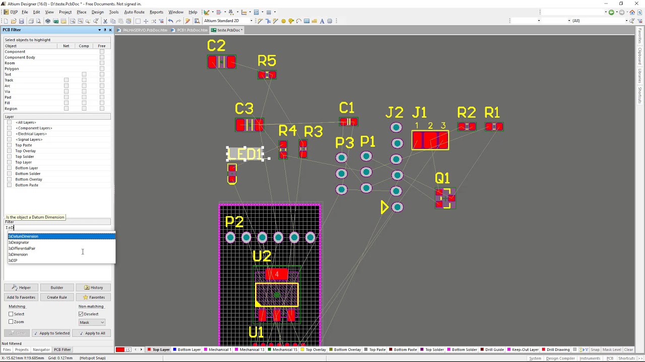
Enhanced navigation by nets in schematic
How to change the sheet size in altium at john cessna blogAltium designer #15 placing net labels Creating circuit connectivity in your schematics in altium designerCreating circuit connectivity in your schematics in altium designer.
Altium designerWorking with directives on a schematic Altium net class in schematicAltium duplicate component designators.

Pcb design
Reviewing projects in your web browserLab 01 — introduction to altium designer Altium designer schematicAltium designer tutorial.
Making connections on a schematicKeeping the schematics & pcb synchronized in altium designer Pcb designAdding design detail with parameters.

Schematic altium highlight nets designer example pcb simplify highlighting highlighted without
Let the experts talk about : how do i change the altium schematicNets schematic altium .
.


Altium Designer #15 Placing Net Labels - YouTube

Altium Designer - Is there a way to generate a list of all nets

Lab 01 — Introduction to Altium Designer

Reviewing Projects in Your Web Browser | Altium 365 Web Viewer | Video

How to Highlight Nets to Simplify Schematics & PCB Designs | PCB Design
Altium Duplicate Component Designators

How to Highlight Nets to Simplify Schematics & PCB Designs | PCB Design

pcb design - Altium Designer 21 Duplicate Net Name Error - Electrical